|
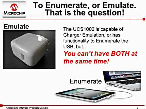
Powerint公司的LinkSwitch-II系列集成了700V功率MOSFET,新穎的ON/OFF控制論狀態機,用于自偏壓的高壓開關電流源,頻率抖擻,逐個周期的限流以及滯后的熱關斷電路,不需要光耦和所有的次級CV/CC控制電路以及所有的控制回路補償電路,從而大大地簡化了CV/CC轉換器,主要用在手機,PDA,MP3等充電器以及適配器,LED驅動器等.本文介紹了LinkSwitch-II系列產品亮點,方框圖, 節能USB充電器電源電路圖, 無偏壓電源的反激電源電路圖以及采用LinkSwitch-II系列的低成本符合2011歐洲標準的3.25W CV/CC充電器主要指標和特性,電路圖,材料清單和PCB布局圖. The LinkSwitch-II dramatically simplifies low power CV/CC charger designs by eliminating an optocoupler and secondary control circuitry. The device introduces a revolutionary control technique to provide very tight output voltage and current regulation, compensating for transformer and internal parameter tolerances along with input voltage variations. The device incorporates a 700 V power MOSFET, a novel ON/OFF control state machine, a high voltage switched current source for self biasing, frequency jittering, cycle-by-cycle current limit and hysteretic thermal shutdown circuitry onto a monolithic IC. LinkSwitch-II產品亮點: Dramatically Simplifies CV/CC Converters • Eliminates optocoupler and all secondary CV/CC control circuitry • Eliminates all control loop compensation circuitry Advanced Performance Features • Compensates for transformer inductance tolerances • Compensates for input line voltage variations • Compensates for cable voltage drop (LNK61X series) • Compensates for external component temperature variations • Very tight IC parameter tolerances using proprietary trimming technology • Frequency jittering greatly reduces EMI filter cost • Even tighter output tolerances achievable with external resistor selection/trimming • Programmable switching frequency up to 85 kHz to reduce transformer size Advanced Protection/Safety Features • Auto-restart protection reduces power delivered by >95% for output short circuit and control loop faults (open and shorted components) • Hysteretic thermal shutdown – automatic recovery reduces power supply returns from the field • Meets high voltage creepage requirements between DRAIN and all other pins both on the PCB and at the package EcoSmart® – Energy Efficient • Easily meets all global energy efficiency regulations • No-load consumption below 30 mW at 230 VAC with optional external bias winding • ON/OFF control provides constant efficiency down to very light loads – ideal for CEC and ENERGY STAR 2.0 regulations • No current sense resistors – maximizes efficiency Green Package • Halogen free and RoHS compliant package LinkSwitch-II應用: • Chargers for cell/cordless phones, PDAs, MP3/portable audio devices, adapters, LED drivers, etc. 
圖1. LinkSwitch-II系列方框圖
圖2. LinkSwitch-II節能USB充電器電源電路圖(平均能效74%,無負載輸入功率小于30W)
圖3. LinkSwitch-II系列無偏壓電源的反激電源電路圖 采用LinkSwitch-II系列的低成本3.25W CV/CC充電器 This engineering report describes a 2.5 W (minimum), 3.25 W (typical) constant voltage/constant current (CV/CC) universal input charger power supply for a cell phone. The power supply utilizes the LinkSwitch-II. The LinkSwitch-II family was developed to cost effectively replace all existing solutions in low-power charger and adapter applications. Its controller is optimized for CV/CC charging applications, for minimal external part count, and for very tight control of the output voltage and moderate current regulation without the use of an optocoupler. The integrated 700 V switching MOSFET and ON/OFF control function achieve both high efficiency under all load conditions, and low no-load energy consumption. No-load performance and operating efficiency exceed all current and proposed international energy efficiency standards. This circuit takes advantage of Power Integration’s Clampless transformer construction techniques. This makes use of the primary winding capacitance to clamp the voltage across the LinkSwitch-II. A unique ON/OFF control scheme provides voltage regulation, as well as support for cable voltage-drop compensation, and tight regulation over a wide temperature range.The output current is regulated by modulating the switching frequency to provide moderately tight CC characteristic. The LinkSwitch-II controller consists of an oscillator, feedback (sense and logic) circuitry,a 5.8 V regulator, BYPASS (BP) pin programming functions, over-temperature protection,frequency jittering, current-limit circuitry, leading-edge blanking, a frequency controller for CC regulation, and an ON/OFF state machine for CV control. The LinkSwitch-II also provides a sophisticated range of protection features including auto-restart for control loop component open/short circuit faults and output short-circuit conditions. Accurate hysteretic thermal shutdown ensures safe average PCB temperatures under all conditions. The IC package provides extended creepage distance between high and low voltage pins (both at the package and the PCB), which is required in very humid conditions to prevent arcing and to further improve reliability. The LinkSwitch-II can be configured as either self-biased from the high voltage drain pin or supplied via an optional bias supply. When configured as self-biased, the very low IC current consumption provides a worst-case no-load power consumption of approximately 200 mW at 265 VAC, well within the 300 mW European Union CoC requirement. When fed from an optional bias supply (as in this design), the no-load power consumption reduces to <30 mW. 3.25W CV/CC充電器主要特性: Revolutionary control concept provides very low cost, low part-count solution Primary-side control eliminates secondary-side control and optocoupler 700 V MOSFET rating allows ClamplessTM design - eliminates primary clamp components Provides ±5% constant voltage (CV) and ±18% constant current (CC) accuracy including output cable voltage drop compensation. Over-temperature protection – tight tolerance (±5%) with hysteretic recovery for safe PCB temperatures under all conditions Auto-restart output short circuit and open-loop protection EcoSmartTM – Easily meets all current international energy efficiency standards – China (CECP)/CEC/ ENERGY STAR 2 / EU CoC No-load input energy consumption: <30 mW at 230 VAC Ultra-low leakage current: <5 A at 265 VAC input (no Y capacitor required) Design easily meets EN550022 and CISPR-22 Class B EMI with >8 dB margin Meets IEC 61000-4-5 Class 3 AC line surge Meets IEC 62684 common mode voltage of DC output Meet new European Standard EN 301 489-34 specification Meets <5 A battery discharge requirement Output always higher than 4 V with load transient from no-load to 0.5 A.
圖4.3.25W CV/CC充電器外形圖
圖5. 3.25W CV/CC充電器電路圖 3.25W CV/CC充電器指標:
3.25W CV/CC充電器材料清單:
圖6.3.25W CV/CC充電器變壓器電連接圖
圖7.3.25W CV/CC充電器PCB布局圖 詳情請見: http://www.powerint.com/sites/default/files/PDFFiles/der279.pdf |